Direct Digital Synthesis (DDS) For Idiots ( like me )
Other names are :
DDFS: Direct Digital Frequency Synthesis:
NCO: Numerically Controlled Oscillator
Introduction
DDS is a method of generating timing signals from a clock source with programmable frequency. It is used in all sorts of places such as frequency hopping, signal synthesis, medical imaging systems, radio receivers, PLLs, test equipment, the list goes on and on. The DDS structure was first proposed in 1971 by Tierney, Josepf, Charles Rader, and Bernard Gold, “A digital frequency synthesizer,” IEEE Transactions on Audio and Electroacoustics.
I have used DDS in a number of places and have found it an easy design, especially for a digital head like me, as the basic DDS much simplifies the analog section of the design. My first design using this technique was an 8 channel audio sinewave generator. One 30k gate FPGA controlled the all 8 of the channels and 4 CODECS did the rest. The performance was excellent – frequency range from 0-20kHz in sub 0.5Hz steps, S/N of better than 90dB and channel separation of better than 90dB. All channels operated independently and were programmed via a USB link to a PC.
What follows is the stuff I find useful when designing a DDS based system. There is much much more that is possible.
Basic DDS Design

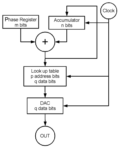
Drawing 1 Basic Vanilla DDS
The basic method works as follows: ( see Drawing 1 Basic Vanilla DDS) The phase register is loaded with a value which is proportional to the required frequency. See Equation 1 Output Frequency.
Then at each rising clock edge the phase register is added to the accumulator.
After enough clocks and additions the accumulator rolls over and starts again from the remainder. That’s all there is for the Numeric Control bit, the rest is output formatting. The top p bits of the accumulator are used to address a lookup table. The lookup table outputs q data bits to the DAC. Which generates the analog output. The anti-a aliasing filter removes all the lumps and bumps, and is fixed at around a third the clock frequency.
Some Basic DDS Equations
See Drawing 1 Basic Vanilla DDS

Equation 1 Output Frequency
where :
n is the number of accumulator bits
Frequency Resolution or what happens if I add one to the phase register

Equation 2 Frequency Resolution
where :
n is the number of accumulator bits
With accumulator sizes of 32 bits or it is easy to get resolutions smaller than 1/2 Hz, even at high frequencies.
Max frequency

Equation 3 Maximum Frequency
where :
m is the number of phase bits
n is the number of accumulator bits
For reasons of practical output filter design, the maximum output frequency is normally limited to Fclk/3. This is so that the max frequency is within the lower passband of the of output anti-aliasing filter. At higher frequencies the signal gets distorted as the output filter peaks before transitioning into the stop band.
If perfect filters were available Fclk/2 would be usable.
Max Phase Jitter
The phase jitter is basically determined by the frequency of the system clock. Although it can be reduced by a neat trick in the analog domain.

Equation 4 Phase Jitter
Signal to quantization noise (SQR )
This is basically a function of how many many bits the DAC has and how much of the range is used.

Equation 5 Quantisation Noise
where :
q = number of bits in the DAC signal is the current signal output level and Max Signal is the full scale output of the DAC.
Over sampling
Oversampling is the use of higher than required sample rates. Minimum rate is defined by Nyquist at 2x the required output frequency, any rate above that is oversampling. Can be used to reduce the effects of quantization noise. Oversampling reduces the effects of quantization noise because quantization energy is spread equally across the bandwidth of the output DAC. By only using a proportion of the the output bandwidth, the quantization noise in the required band is reduced.

Equation 6 Reduction in Quantisation Noise due to Oversampling
where :
q = number of bits in the DAC signal is the current signal output level and Max Signal is the full scale output of the DAC.
Accumulator Truncation
Errors are added to the output signal due to the truncation of the accumulator before the look up table. Causes spurs in the frequency domain at multiples of the output frequency. Spurs vary from 0 to maximum truncation error shown below.
Assume accumulator is n bits.
Look up table address is p bits
If n – p is >=4 then
Equation 7 Truncation Errors
Other Error Sources
There are a number of other sources of errors and noise in a DDS system. Some are outlined below.
DAC linearity
Basically this is a measure of whether each increment of the digital data causes a consistent increment in the analog output.
DAC switching transients
All DACS show a step response when the input digital data changes. This causes switching transients to appear on the output.
Clock feed through.
This will mainly be down to power supply and layout issues. Take care to provide enough decoupling on the power supplies to all the devices and that the PCB layout is sympathetic to getting low noise analog outputs.
Some other stuff to know
Clock Jitter – reduced by switching to the analog world then back to digital!!
Rather neat this – a DDS can reduce the jitter from the base clock frequency. The incoming clock will have a jitter component, this shows up in the output signal as a frequency components above the fundamental of the required output. By filtering these jitter components to say 50dB below the required fundamental frequency, the jitter component in the output is reduced.
Lookup Table considerations
If used for sinewave generating then the lookup table can be shortened, as a sinewave is four way symmetrical. So the table only needs to store a single quadrant of data, then with a bit of simple data manipulation all values can be found. This reduces the lookup table requirements by a factor of 4. So we can have either a smaller table or have more resolution.
The lookup table needs to be accessed at the system clock rate.
Could use interpolation to improve the resolution of a lookup table.
Lookup tables can be designed out completely by the use of various techniques such as CORDIC or the Taylor series. This is a bit beyond the scope of this introductory article though.
DAC and Analog Stages
The main thing about the DAC is the update rate must cope with the system clock speed not the required output frequency. This is the main limitation of a DDS system.
The analog stage is easily designed as the system clock is at least three times the required output frequency. Also compared to other signal generation techniques the system clock frequency is constant. Thus much simplifying any filter design for the output stage.
Easy things you can do with a DDS
Frequency Shift Keying (FSK ) /Frequency Modulation (FM)/Frequency Hopping
Changing the phase register changes the frequency. So FSK can be implemented by simply changing the phase register between two values.
Alternatively two phase registers can be used with a multiplexer to select the register which is used. More sophisticated versions would allow for a gentle change between two or more values, possibly under microprocessor control. Or using a table of values to implement a frequency hopping system.
The speed of change is basically down to how fast the phase register can be altered.
Changing the frequency does not affect the phase of the output signals.
The big advantage is that the frequency change creates no discontinuities in the output waveform.
Frequency Sweep
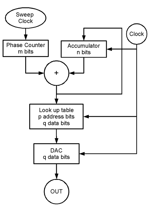
Very similar to the FSK system, by making phase register the output of a clocked counter, the output frequency can be made to sweep at the rate of the sweep clock. With the advantages of no phase shifting or discontinuities on change.

Drawing 2 DDS System With Frequency Sweeping
PSK Phase shift Keying
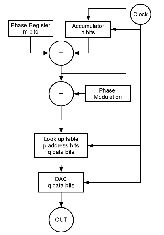
Adding a fixed offset to the output of the accumulator is the equivalent to adding a fixed phase offset. By changing the amount added the phase of the output signal is varied. This can be done as using a simple register or multiple registers or look up tables.
Gives excellent phase shift resolution.

Drawing 3 DDS with Phase Modulation
Phase Dithering To Reduce SFDR Whats SFDR ? It’s the spurious free dynamic range.
It is a measure of the power of the required frequency against the power of the largest noise source in the signal. Typically this noise is at a frequency multiple of the required frequency.
By using the techniques described in the phase modulation, you can trade over system noise performance against SFDR. Basically by adding a small amount of random phase noise to the DDS system, the coherence of the noise signals is reduced. This can reduce the SFDR by upto 12dB.
Amplitude Modulation (AM )
Can be done digitally by implementing a digital multiplier, after the lookup table, or in analog fashion by manipulating the gain of the output signal.
Beware though if implemented digitally, the DAC won’t be used over its full operating range at all times. Thus the SQR figure will vary depending on the amplitude.
Also the multiplier will need to run at the same frequency as the accumulator, which may restrict the maximum frequency the DDS can run at. ( Note some FGPAs now include hardware multiplier blocks which make this much easier to implement. )
Some other ways of AM modulating the signal are :
- use a multiplying DAC.
- change the DAC reference voltage dynamically.
- use an analog switched attenuation stage.
Arbitrary Function Generator
If the lookup table is filled with values from an arbitrary periodic waveform, then the output will be that waveform at the required frequency. This may need a higher specification DAC and analog stage.
Implementing DDS systems
There are numerous ways of implementing a DDS. There are discrete DDS ICs available, it is a easy shoe into an FPGA and it can even be done in software. My favourite is the FPGA route, just for the flexibility it gives. Several of the FPGA vendors supply DDS IP, but I find it just as easy to roll my own. See below for some simple sample VHDL code.
Simple VHDL Implementation
— following code will output a binary ramp or sequential values from a lookup table at a frequency – proportional to the value in the phase reg.
— the signal ramp selects the ramp output or the sinewave output.
library ieee;
use ieee.std_logic_1164.all;
entity dds is
port(
clk : in std_logic;
reset : in std_logic;
phasereg : in std_logic_vector( 27 downto 0 );
ramp : in std_logic;
data : out std_logic_vector( 11 downto 0 )
);
end entity dds;
architecture rtl of dds is
component lookuptable is
port(
clk : in std_logic;
reset : in std_logic;
addr : in std_logic_vector( 11 downto 0);
data : out std_logic_vector( 11 downto 0)
);
end component lookuptable;
signal accumulator : std_logic_vector( 31 downto 0 );
signal iphasereg : std_logic_vector( 31 downto 0 );
signal lookuptabledata : std_logic_vector( 11 downto 0 );
begin
— this just makes the math a bit easier to look at later on.
iphasereg <= x”0″ & phasereg;
— process adds phase reg to accumulator every clock – the basic oscillator part of the dds.
l_dds : process ( clk, reset, i_phase_reg, accumulator)
begin
if ( reset =’1′ ) then
accumulator <= x”00000000″;
else
if (rising_edge(clk) ) then
accumulator <= accumulator + i_phase_reg;
end if;
end if;
end process;
— select either a ramp waveform or data from the lookuptable.
data <= accumulator (31 downto 20 ) when ramp =’1′
else
lookuptabledata;
— instantiate the lookup table
— assumes a 4096 entry lookup table with each entry being 12 bits wide.
— adjust values to suit
— typically would fill with sinewave values – but could be any periodic waveform.
— best if synchronous
l_lookup_table: lookuptable
( port map
clk <= clk,
reset <= reset,
addr <= accumulator( 31 downto 20 ),
data <= lookuptabledata
);
end architecture dds;
Linkages and further reading
DDS links
Altera IP based DDS
Analog Devices Web site for discrete DDS ICs
Analog Devices Tutorial
EDN Article On DDS
Jesper’s AVR pages – MiniDDS – DDS in software.
Xilinx Frequency synthesis App Note
CORDIC Links
Andraka’s CORDIC in FPGAs
The maths involved or – “Fixed Point Trigonometry with CORDIC Iterations” by Ken Turkowski
Open Cores Implemenatation
